Industrialization of Perovskite-Silicon Photovoltaics: New Progress
The production of the first perovskite-silicon tandem solar panels has officially begun, but it still seems premature to talk about a trend or niche technology in the market. Beyond the pioneering work conducted by Oxford PV, perovskite-silicon photovoltaics continue to struggle to integrate into existing production lines. The main issue? Successfully industrializing the method of depositing the perovskite layer to obtain a stable, durable, and economically competitive product.
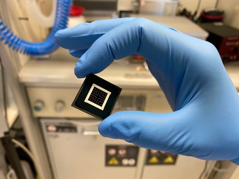
In general, industry experts believe that large-scale production could be achieved within the next ten years. However, various industry research efforts are trying to shorten this timeline. One such effort comes from scientists at the Fraunhofer Institute for Solar Energy Systems ISE in Germany. The group, led by Dr. Juliane Borchert, has employed a new approach to produce a textured perovskite-silicon tandem solar cell of 1 cm² with an efficiency of 31.6%.
This is a significant achievement as the top perovskite layer has been directly deposited on an industrially textured silicon heterojunction solar cell.
Perovskite-Silicon Photovoltaics: How It Works
Perovskite-silicon photovoltaics consist of a lower crystalline silicon cell that converts the less energetic part of the solar spectrum and an upper layer made of perovskites optimized to convert the more energetic part of the spectrum.
This combination is theoretically perfect. Crystalline silicon remains the number one material in the solar energy market today, thanks to its efficiency, reliability, and technological maturity. Perovskite, on the other hand, is much more effective at absorbing light and can be specifically “tuned” to utilize regions of the solar spectrum that are largely inaccessible to silicon photovoltaics.
However, for this to transform into a successful commercial product, perovskite-silicon tandem photovoltaic modules must demonstrate an efficiency greater than 32%. They also need to keep production costs within a certain upper limit (estimated at no more than 30% compared to traditional photovoltaics).
On the efficiency front, progress is evident: the current record for converting light into electricity for this type of photovoltaic technology belongs to Longi, which in October 2023 presented a perovskite-Si solar cell of 1 cm² with an efficiency of 33.9%.
Increasing Yield to Cut Costs
On the cost front, the competition is still open. The main goals are to deposit perovskite on textured silicon successfully. Industrial c-Si solar cells have a surface structure made up of microscopic pyramids. These features help direct more light into the solar cell, reducing reflection losses. Using this industrial standard as a base for perovskite-silicon multi-junction architectures would lead to higher energy yields and make integration into established production processes easier.
The research from Fraunhofer ISE paves the way. The scientists have developed a tandem unit by depositing the perovskite layer on an industrially textured silicon heterojunction solar cell using a hybrid approach.
“The pyramidal surface of silicon solar cells, however, poses a challenge for the second sub-cell of the tandem,” explains Borchert. “To apply the perovskite layer uniformly on such a surface structure, a special method is necessary. Here, we are working on a combined hybrid process of vapor deposition and wet chemical deposition.”
The Efficiency Record of Textured Perovskite-Silicon Photovoltaics
The result speaks for itself. The textured perovskite-silicon photovoltaic developed by Fraunhofer ISE boasts an efficiency of 31.6%—certified by CalLab—which represents the highest value ever achieved using a silicon solar cell with an industrial structure.
“To achieve this result, we focused on the upper perovskite cell and specifically optimized the passivation between the perovskite layer and the electron transport layer,” adds Borchert. “We anticipate that further efficiency increases will be possible by improving the lower silicon cell.”